HCLTech’s Advanced Semiconductor Lab Begins Commercial Programmes to Support India’s Semiconductor Ecosystem
HCL Tech has already executed commercial semiconductor programmes at its recently commissioned Bengaluru Advanced Semiconductor Lab, with the facility designed to support fabless companies, startups and global customers through post-silicon engineering, advanced testing and failure analysis.
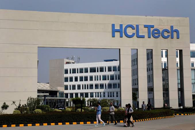
Noida-headquartered HCLTech has started executing commercial programmes at its newly commissioned Advanced Semiconductor Lab in Bengaluru, with the company positioning the facility as a shared infrastructure platform for Indian fabless semiconductor companies, startups and global customers.
Ameer Saithu, Executive Vice President & Head of Global Semiconductor Business at HCLTech, said the company is already serving customers through the facility, including global customers that have used the lab to test their upcoming semiconductor intellectual property (IP).
The company has invested ₹185 crore in establishing the lab, which includes 25,000 sq ft of Class 10K and Class 1K cleanrooms. The facility is designed to provide end-to-end post-silicon engineering, advanced semiconductor testing, failure analysis and new product introduction (NPI) capabilities.
The laboratory is equipped with semiconductor and RF test and analysis infrastructure from global technology providers including Teradyne, Advantest, Keysight Technologies, Tektronix and Thermo Fisher Scientific. These capabilities are intended to support activities ranging from R&D and pre-production to production qualification.
For India's growing fabless semiconductor ecosystem, one of the key advantages of the facility is its as-a-service model. HCLTech says companies can access capital-intensive semiconductor testing and qualification infrastructure without having to make large investments in their own equipment, which could be particularly useful for startups and lower-volume programmes.
The development comes as India sees increasing private-sector investment across semiconductor design, manufacturing, assembly and testing. HCLTech's semiconductor strategy extends beyond testing infrastructure, with the company looking to act as a co-development partner for customers across application areas such as telecom networking, healthcare, automotive and other industry-specific silicon applications.
According to Saithu, semiconductor applications are becoming increasingly domain-specific, creating an opportunity for HCLTech to combine its existing engineering and industry expertise with silicon development capabilities.
HCLTech is also part of the broader semiconductor manufacturing push in India through India Chip Private Limited, a joint venture between the HCL Group and Foxconn that is establishing an OSAT facility in Jewar, Greater Noida, with an investment of more than ₹23,700 crore.
For RF, analog and semiconductor engineers in India, the Bengaluru lab could become an important piece of local infrastructure by bringing advanced ATE, RF instrumentation, post-silicon validation and failure-analysis capabilities closer to domestic design teams.
As India moves from semiconductor design toward commercial deployment and manufacturing, access to such shared infrastructure could help Indian startups and fabless companies shorten development cycles and reduce the cost of taking silicon from tape-out to qualified product.