Semicon India 2.0: India Shifts From Semiconductor Capacity Creation to Ecosystem Leadership
India’s Semicon 2.0 program expands the country’s semiconductor strategy beyond fabs and packaging toward a six-pillar ecosystem covering design, machines and materials, fabrication, advanced packaging, R&D and talent development, backed by an outlay of ₹1,27,500 crore.
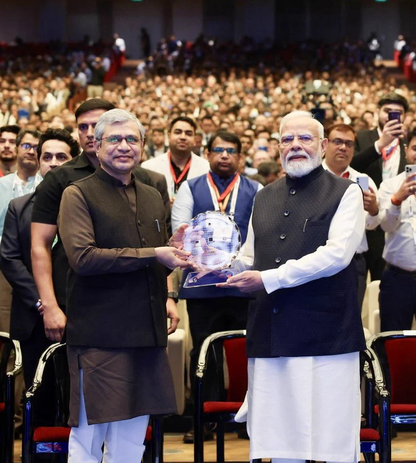
India’s semiconductor strategy is entering a new phase. After using Semicon India 1.0 to establish foundational capabilities in chip design, fabrication and packaging, the Government of India launched Semicon India 2.0 in July 2026 with an enhanced outlay of ₹1,27,500 crore (about US$13.3 billion). The central shift is from creating individual manufacturing capacity to developing a deeper, interconnected semiconductor ecosystem.
According to the EY–India Electronics and Semiconductor Association (IESA) report, Semicon India 1.0 was launched with an outlay of ₹76,000 crore. By 2026, India had approved 12 semiconductor manufacturing projects: one silicon fab, two compound-semiconductor fabs and nine packaging facilities, representing cumulative investments of roughly ₹1.64 lakh crore. The report also notes 23 completed chip tape-outs and says three semiconductor units had already commenced production and exports.
This progress is occurring alongside rapid growth in domestic semiconductor demand. The report estimates that India’s semiconductor market grew from approximately US$27 billion in 2021 to around US$64 billion in 2026 and projects it could reach US$200 billion by 2035. India also has a major semiconductor-design base, with the report citing nearly 20% of the world’s chip-design engineers as being based in the country.
Semicon 2.0 broadens the policy framework around six pillars: Design; Machines and Materials; Fabrication; Assembly, Testing, Marking and Packaging (ATMP/OSAT); Research and Development; and Talent Development. This recognizes that semiconductor competitiveness depends not only on building fabs, but also on the surrounding design IP, equipment, materials, packaging, research infrastructure, skilled workforce and commercialization capabilities.
For semiconductor design companies, startups and MSMEs, the program is intended to lower barriers to innovation and commercialization through access to advanced design infrastructure, EDA tools, IP cores, multi-project wafer services, seed funding, equity participation and enhanced deployment-linked incentives. The broader objective is to translate India’s existing engineering and design strength into greater ownership of semiconductor IP and commercially scalable products.
The policy also gives greater attention to the upstream supply chain. Dedicated support for semiconductor-grade materials, specialty chemicals, gases, substrates, equipment and testing infrastructure is intended to deepen domestic value addition and reduce dependence on imported inputs. For fabrication, support continues across silicon and compound-semiconductor technologies, while advanced packaging receives specific attention as chiplets, heterogeneous integration and 2.5D/3D packaging become increasingly important.
The report highlights compound and wide-bandgap semiconductors as part of this technology landscape. Silicon carbide (SiC) and gallium nitride (GaN) are identified as important materials for power-electronics applications, while GaN also has high-frequency applications. Gallium arsenide (GaAs) is highlighted for selected high-frequency and optoelectronic uses, including RF amplifiers. This is particularly relevant to India’s emerging RF, power-electronics, defence, telecom and advanced electronics ecosystem.
R&D and talent development are treated as distinct pillars under Semicon 2.0. Eligible initiatives may receive support of up to 75% of project costs, including state incentives. The report emphasizes practical workforce development across design, fabs, packaging, testing, equipment, materials, cleanrooms and infrastructure, as well as shared R&D platforms that can serve universities, startups, companies and research organizations.
EY and IESA argue that the next stage will ultimately be determined by execution and ecosystem depth. Their roadmap points to opportunities such as better alignment of state semiconductor policies, semiconductor-specific fiscal measures, simpler business and customs processes, integrated manufacturing clusters, dedicated talent-certification programs and a national semiconductor research and commercialization platform modeled on institutions such as Taiwan’s ITRI or Belgium’s imec.
The report’s larger message is that India is moving beyond semiconductor ambition toward semiconductor execution. Semicon 2.0 is designed to connect design, manufacturing, packaging, suppliers, R&D and talent into a more complete domestic value chain. If policy momentum is converted into technology commercialization, indigenous IP, capable suppliers, skilled talent and globally competitive manufacturing, India’s semiconductor opportunity could extend well beyond capacity creation into sustained ecosystem participation and leadership.
Key numbers:
₹1,27,500 crore — Semicon India 2.0 outlay ₹76,000 crore — Semicon India 1.0 outlay 12 — semiconductor manufacturing projects approved under the first phase ₹1.64 lakh crore — approximate cumulative investment in approved projects 23 — chip tape-outs completed US$64 billion — estimated Indian semiconductor market in 2026 US$200 billion — projected Indian semiconductor market by 2035 Up to 75% — project-cost support cited for eligible R&D and talent-development initiatives
What do you think of India's semiconductor mission's Semicon 2.0 outlay and EY-IESA's report?